

Xinghe Da Technology Co., Ltd
Contacts:Jack Peng
Mobile:+86 18627553022
Whatsapp:+86 18627553022
WeChat: pengyi-changsha
E-mail:admin@chinaxingheda.com
Company address :2506 Xidi Building, No. 8 Fenglin Third Road, Yuelu District, Changsha City, Hunan Province
OLT,XPON-HUAWEI SL1DA-SL91 2xSTM-1 interface board
Application
SL1D SL1DA boards help OptiX RTN 980 NEs converge TDM services from radio networks before forwarding the services to SDH networks, or help OptiX RTN 980 NEs build SDH networks together with SDH equipment
Converging TDM Services from Radio Networks
SL1D SL1DA boards converge TDM services from radio networks before forwarding the services to SDH networks
Figure 1 Application scenario of SL1D SL1DA boards (1)
Product Details:
Version Description
The functional version of the SL1D/SL1DA is SL91.
Application
SL1D/SL1DA boards help OptiX RTN 980 NEs converge TDM services from radio networks before forwarding the services to SDH networks, or help OptiX RTN 980 NEs build SDH networks together with SDH equipment.
Converging TDM Services from Radio Networks
SL1D/SL1DA boards converge TDM services from radio networks before forwarding the services to SDH networks.
Figure 1 Application scenario of SL1D/SL1DA boards (1)
NOTE:
Converged services shown in the preceding figure can be SDH/PDH services from TDM radio networks or native E1/STM-1 services from IP radio networks.
Transmission lines between the OptiX RTN equipment and the SDH network can be configured with linear MSP.
OptiX RTN 980 NEs can work as nodes on SDH rings, as shown in Figure 2. Services on such SDH rings can be configured with SNCP.
Figure 2 Application scenario of SL1D/SL1DA boards (2)
Helping OptiX RTN 980 NEs Build SDH Networks Together with SDH Equipment
OptiX RTN 980 NEs using SL1D/SL1DA boards can build SDH networks together with SDH equipment. In this scenario, radio links function as dark fibers.
Figure 3 Application scenario of SL1D/SL1DA boards (3)
NOTE:
IF boards shown in the preceding figure can be TDM IF boards working in SDH radio mode, or general-purpose IF boards or XPIC IF boards working in SDH radio or native STM-1+Ethernet mode.
SL1DA boards must be installed if K bytes need to be transparently transmitted.
Radio links can form SDH rings together with SDH fiber links. Services on such SDH rings can be configured with SNCP.
Functions and Features
An SL1D/SL1DA receives and transmits 2xSTM-1 optical/electrical signals.
Table 1 lists the functions and features that the SL1D/SL1DA supports.
Table 1 Functions and features that the SL1D/SL1DA supports
NOTE:
a: The ALS function is implemented as follows:
After an optical module detects an R_LOS alarm at its receive port and the alarm persists for 500 ms, the laser at the specific transmit port is automatically shut down.
The laser starts to launch laser pulses at a specified interval; that is, the laser emits light for 2s and stops emission for 60s.
After the R_LOS alarm is cleared, the laser restarts to work properly and emits continuous light.
Working Principle and Signal Flow
This section describes how to process one STM-1 optical signal, and it serves as an example to describe the working principle and signal flow of the SL1D/SL1DA.
Functional Block Diagram
Figure 1 Functional block diagram of the SL1D/SL1DA
Signal Processing in the Receive Direction
Table 1 Signal processing in the receive direction of the SL1D/SL1DA
Signal Processing in the Transmit Direction
Table 2 Signal processing in the transmit direction of the SL1D/SL1DA
Control Signal Processing
The board is directly controlled by the CPU unit on the system control and communication unit. The CPU unit issues configuration and query commands to the other units of the board over the control bus. These units then report command responses, alarms, and performance events to the CPU unit over the control bus.
The logic control unit decodes the address read/write signals from the CPU unit of the system control and communication unit and enables FPGA loading.
Clock Unit
This unit receives the system clock from the control bus in the backplane and provides clock signals to the other units on the board.
Front Panel
There are indicators, STM-1 ports, and a label on the front panel.
Front Panel Diagram
Figure 1 Front panel of the SL1D (with optical ports)
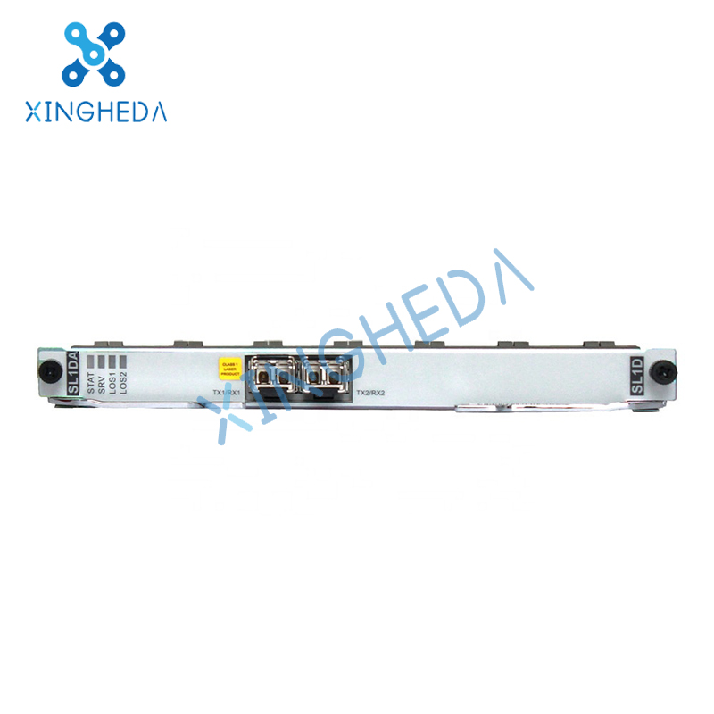
Figure 2 Front panel of the SL1DA (with optical ports)
Figure 3 Front panel of the SL1D (with electrical ports)
Figure 4 Front panel of the SL1DA (with electrical ports)
Indicators
Table 1 Status explanation for indicators on the SL1D/SL1DA
The functional version of the SL1D/SL1DA is SL91.
Application
SL1D/SL1DA boards help OptiX RTN 980 NEs converge TDM services from radio networks before forwarding the services to SDH networks, or help OptiX RTN 980 NEs build SDH networks together with SDH equipment.
Converging TDM Services from Radio Networks
SL1D/SL1DA boards converge TDM services from radio networks before forwarding the services to SDH networks.
Figure 1 Application scenario of SL1D/SL1DA boards (1)
NOTE:
Converged services shown in the preceding figure can be SDH/PDH services from TDM radio networks or native E1/STM-1 services from IP radio networks.
Transmission lines between the OptiX RTN equipment and the SDH network can be configured with linear MSP.
OptiX RTN 980 NEs can work as nodes on SDH rings, as shown in Figure 2. Services on such SDH rings can be configured with SNCP.
Figure 2 Application scenario of SL1D/SL1DA boards (2)
Helping OptiX RTN 980 NEs Build SDH Networks Together with SDH Equipment
OptiX RTN 980 NEs using SL1D/SL1DA boards can build SDH networks together with SDH equipment. In this scenario, radio links function as dark fibers.
Figure 3 Application scenario of SL1D/SL1DA boards (3)
NOTE:
IF boards shown in the preceding figure can be TDM IF boards working in SDH radio mode, or general-purpose IF boards or XPIC IF boards working in SDH radio or native STM-1+Ethernet mode.
SL1DA boards must be installed if K bytes need to be transparently transmitted.
Radio links can form SDH rings together with SDH fiber links. Services on such SDH rings can be configured with SNCP.
Functions and Features
An SL1D/SL1DA receives and transmits 2xSTM-1 optical/electrical signals.
Table 1 lists the functions and features that the SL1D/SL1DA supports.
Table 1 Functions and features that the SL1D/SL1DA supports
| Function and Feature | Description | |
| Basic functions | Receives and transmits 2xSTM-1 optical/electrical signals. | |
| Port specifications | Optical ports | Uses SFP optical modules to provide optical ports of Ie-1, S-1.1, L-1.1, and L-1.2 types. Provides ITU-T G.957-compliant optical port specifications. |
| Electrical ports | Adopts SFP electrical modules. The performance of the electrical ports complies with ITU-T G.703. |
|
| Protection | LMSP | Supported |
| SNCP | Supported | |
| Clock | Clock source | Provides one SDH line clock signal over each line port. |
| Clock protection | Supports the following clock protection schemes: Protection based on clock source priorities Protection by running the SSM protocol Protection by running the extended SSM protocol |
|
| Data communication network (DCN) | Outband DCN | Provides a 3-, 9-, or 12-byte DCC channel over each SDH line port. |
| K byte pass-through | Supported only by the SL1DA | |
| OM | Loopback | Supports the following loopback types: Outloops at optical/electrical ports Inloops at optical/electrical ports Outloops on VC-4 paths Inloops on VC-4 paths |
| Warm reset and cold reset | Supported | |
| Setting of the on/off state of a laser | Supported | |
| ALS functiona | Supported | |
| In-service FPGA loading | Supported | |
| Queries of board manufacturing information | Supported | |
| Queries of the board power consumption | Supported | |
| Detection and query of SFP module information | Supported | |
a: The ALS function is implemented as follows:
After an optical module detects an R_LOS alarm at its receive port and the alarm persists for 500 ms, the laser at the specific transmit port is automatically shut down.
The laser starts to launch laser pulses at a specified interval; that is, the laser emits light for 2s and stops emission for 60s.
After the R_LOS alarm is cleared, the laser restarts to work properly and emits continuous light.
Working Principle and Signal Flow
This section describes how to process one STM-1 optical signal, and it serves as an example to describe the working principle and signal flow of the SL1D/SL1DA.
Functional Block Diagram
Figure 1 Functional block diagram of the SL1D/SL1DA
Signal Processing in the Receive Direction
Table 1 Signal processing in the receive direction of the SL1D/SL1DA
| Step | Function Unit | Processing Flow |
| 1 | O/E conversion unit | Regenerates STM-1 optical signals. Detects R_LOS alarms. Converts STM-1 optical signals into electrical signals. |
| 2 | Overhead processing unit | Restores clock signals. Aligns frames and detects R_LOS and R_LOF alarms. Performs descrambling. Checks B1 and B2 bytes and generates specific alarms and performance events. Checks the M1 byte and bits 6-8 of the K2 byte, and generates specific alarms and performance events. Detects the changes in the SSM in the S1 byte and reports the SSM status to the system control and communication unit. Extracts orderwire bytes, auxiliary channel bytes including F1 and SERIAL bytes, DCC bytes, and K bytes and transmits the overhead signal to the logic processing unit. Adjusts AU pointers and generates specific performance events. Checks higher order path overheads and generates specific alarms and performance events. Transmits VC-4 signals and pointer indication signals to the logic processing unit. |
| 3 | Logic processing unit | Processes clock signals. Ttransmits the overhead signals to the system control and communication unit. Transmits VC-4 signals and pointer indication signals to the cross-connect unit. |
Table 2 Signal processing in the transmit direction of the SL1D/SL1DA
| Step | Function Unit | Processing Flow |
| 1 | Logic processing unit | Processes clock signals. Processes overhead signals. Receives VC-4 signals and pointer indication signals from the cross-connect unit. |
| 2 | Overhead processing unit | Sets higher order path overheads. Sets AU pointers. Sets multiplex section overhead bytes. Sets regenerator section overhead bytes. Performs scrambling. |
| 3 | O/E conversion unit | Converts electrical signals into optical signals. |
The board is directly controlled by the CPU unit on the system control and communication unit. The CPU unit issues configuration and query commands to the other units of the board over the control bus. These units then report command responses, alarms, and performance events to the CPU unit over the control bus.
The logic control unit decodes the address read/write signals from the CPU unit of the system control and communication unit and enables FPGA loading.
Clock Unit
This unit receives the system clock from the control bus in the backplane and provides clock signals to the other units on the board.
Front Panel
There are indicators, STM-1 ports, and a label on the front panel.
Front Panel Diagram
Figure 1 Front panel of the SL1D (with optical ports)
Figure 2 Front panel of the SL1DA (with optical ports)
Figure 3 Front panel of the SL1D (with electrical ports)
Figure 4 Front panel of the SL1DA (with electrical ports)
Indicators
Table 1 Status explanation for indicators on the SL1D/SL1DA
A Free Consultation
You can contact us any way that is convenient for you. We are available 24/7 via fax, email or telephone.