

Xinghe Da Technology Co., Ltd
Contacts:Jack Peng
Mobile:+86 18627553022
Whatsapp:+86 18627553022
WeChat: pengyi-changsha
E-mail:admin@chinaxingheda.com
Company address :2506 Xidi Building, No. 8 Fenglin Third Road, Yuelu District, Changsha City, Hunan Province
OLT,XPON-HUAWEI ML1 SL91 16xE1 (Smart) tributary board
Product Description
The functional version of the ML1 is SL92 The functional version of the MD1 is SL91
Application
ML1 MD1 boards receive and transmit E1 services on OptiX RTN 910 NEs that transmit E1-carried ATM CES services in PWE3 mode The selection of MD1 or ML1 boards depends on desired port quantities
NOTE:
For the OptiX RTN 910, configure ML1
Product Details:
Product Description
The functional version of the ML1 is SL92. The functional version of the MD1 is SL91.
Application
ML1/MD1 boards receive and transmit E1 services on OptiX RTN 910 NEs that transmit E1-carried ATM/CES services in PWE3 mode. The selection of MD1 or ML1 boards depends on desired port quantities.
NOTE:
For the OptiX RTN 910, configure ML1/MD1 boards only if Smart E1 ports on system control, switching, and timing boards cannot meet customers' requirements.
The ML1/MD1 board are used to:
Transmit CES/ATM E1 services in PWE3 mode.
Allow an MPLS tunnel to traverse a TDM network
Transmitting CES/ATM E1 Services in PWE3 Mode
Figure 1 Transmitting CES/ATM E1 services in PWE3 mode
Allowing an MPLS Tunnel to Traverse a TDM Network
Figure 2 Allowing an MPLS tunnel to traverse a TDM network
NOTE:
IF boards shown in Figure 1 and Figure 2 must be general-purpose IF boards or XPIC IF boards working in native E1+Ethernet mode or native STM-1+Ethernet mode.
Functions and Features
The ML1 receives and transmits 16xE1 signals. The MD1 receives and transmits 32xE1 signals.
Table 1 lists the functions and features that the ML1/MD1 supports.
Table 1 Functions and features
Working Principle and Signal Flow
This section describes how to process one E1 signal, and it serves as an example to describe the working principle and signal flow of the ML1/MD1.
Functional Block Diagram
Figure 1 Functional block diagram of the ML1/MD1
Signal Processing in the Receive Direction
Table 1 Signal processing in the receive direction of the ML1/MD1
Signal Processing in the Transmit Direction
Table 2 Signal processing in the transmit direction of the ML1/MD1
Control Signal Processing
The board is directly controlled by the CPU unit on the system control and communication unit. The CPU unit issues configuration and query commands to the other units of the board over the control bus. These units then report command responses, alarms, and performance events to the CPU unit over the control bus.
The logic control unit decodes the address read/write signals from the CPU unit of the system control and communication unit.
Power Supply Unit
The power supply unit performs the following functions:
Receives two -48 V power supplies from the backplane, converts the -48 V power supplies into +3.3 V power, and then supplies the +3.3 V power to the other units on the board.
Receives one +3.3 V power supply from the backplane, which functions as a +3.3 V power backup for the other units on the board.
Clock Unit
This unit receives the system clock from the control bus in the backplane and provides clock signals to the other units on the board.
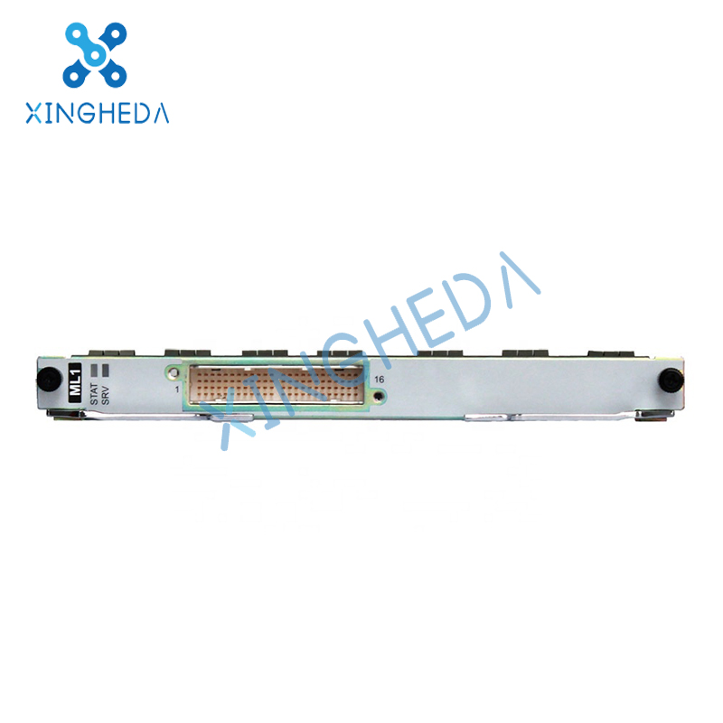
Front Panel
There are indicators and E1 ports on the front panel.
Front Panel Diagram
Figure 1 Front panel of the ML1
Figure 2 Front panel of the MD1
The functional version of the ML1 is SL92. The functional version of the MD1 is SL91.
Application
ML1/MD1 boards receive and transmit E1 services on OptiX RTN 910 NEs that transmit E1-carried ATM/CES services in PWE3 mode. The selection of MD1 or ML1 boards depends on desired port quantities.
NOTE:
For the OptiX RTN 910, configure ML1/MD1 boards only if Smart E1 ports on system control, switching, and timing boards cannot meet customers' requirements.
The ML1/MD1 board are used to:
Transmit CES/ATM E1 services in PWE3 mode.
Allow an MPLS tunnel to traverse a TDM network
Transmitting CES/ATM E1 Services in PWE3 Mode
Figure 1 Transmitting CES/ATM E1 services in PWE3 mode
Allowing an MPLS Tunnel to Traverse a TDM Network
Figure 2 Allowing an MPLS tunnel to traverse a TDM network
NOTE:
IF boards shown in Figure 1 and Figure 2 must be general-purpose IF boards or XPIC IF boards working in native E1+Ethernet mode or native STM-1+Ethernet mode.
Functions and Features
The ML1 receives and transmits 16xE1 signals. The MD1 receives and transmits 32xE1 signals.
Table 1 lists the functions and features that the ML1/MD1 supports.
Table 1 Functions and features
| Function and Feature | Description | ||
| ML1 | MD1 | ||
| Basic functions | Receives and transmits E1 signals, and supports flexible configuration of E1 service categories. | ||
| E1 service categories | Supports the following E1 service categories: CES E1 ATM/IMA E1 ML-PPP E1 |
||
| Port specifications | 75-ohm/120-ohm E1 port | 16 | 32 |
| Fractional E1 | Supports transparent service transmission at the 64 kbit/s level. | ||
| ATM/IMA | Maximum number of ATM services | 64 | |
| Maximum number of ATM connections | 256 | ||
| ATM traffic management | Supported | ||
| ATM encapsulation mode | Supports the following ATM encapsulation modes: N-to-one VPC N-to-one VCC One-to-one VPC One-to-one VCC |
||
| Maximum number of concatenated ATM cells | 31 | ||
| ATM OAM | Supports F4 OAM (VP level) and F5 OAM (VC level), including the following functions: Alarm indication signal (AIS)/Remote defect indication (RDI) Continuity check test Loopback test |
||
| Maximum number of IMA groups | 16 | 32 | |
| Maximum number of members in an IMA group | 16 | ||
| CES | Maximum number of services | 16 | 32 |
| Encapsulation mode | Supports the following encapsulation modes: CESoPSN SAToP |
||
| Service category | Point-to-point services | ||
| Compression of vacant slots | Supported (applicable to CESoPSN only) | ||
| Jitter buffering time (us) | 375-16000 | ||
| Packet loading time (us) | 125-5000 | ||
| CES ACR | Supported | ||
| Retiming | Supported | ||
| MLPPP | MLPPP link type | E1 | |
| Maximum number of PPP links | 16 | 32 | |
| Maximum number of MLPPP groups | 8 | 16 | |
| Maximum number of links in an MLPPP | 16 | ||
| Clock | Clock source | Supports a tributary clock source extracted from the first or fifth E1 signal. | |
| Clock protection | Supports clock protection based on clock source priorities. | ||
| E1 retiming function | Supported | ||
| OM | Loopback | Supports inloops and outloops at E1 tributary ports. | |
| Cold reset and warm reset | Supported | ||
| PRBS tests at E1 ports | Supported | ||
| Board manufacturing information query | Supported | ||
| Board power consumption information query | Supported | ||
Working Principle and Signal Flow
This section describes how to process one E1 signal, and it serves as an example to describe the working principle and signal flow of the ML1/MD1.
Functional Block Diagram
Figure 1 Functional block diagram of the ML1/MD1
Signal Processing in the Receive Direction
Table 1 Signal processing in the receive direction of the ML1/MD1
| Step | Function Unit | Processing Flow |
| 1 | Signal interface unit | Receives external E1 signals. Matches the resistance. Equalizes signals. Converts the level. Recovers clock signals. Buffers the received data. Performs HDB3 decoding. |
| 2 | Service processing unit | Frames E1 signals. Performs CES emulation or processes ATM/IMA services. Encapsulates PWE3 services and converts the PWE3 services into Ethernet services. |
| 3 | Logic processing unit | Implements the conversion from the internal service bus into the GE bus in the backplane. Sends service signals to the packet switching unit. |
Table 2 Signal processing in the transmit direction of the ML1/MD1
| Step | Function Unit | Processing Flow |
| 1 | Logic processing unit | Receives service signals from the packet switching unit. Implements the conversion from the GE bus in the backplane into the internal service bus. |
| 2 | Service processing unit | Decapsulates service signals. Re-forms CES packets or processes ATM/IMA services. Converts signals into E1 signals and sends the E1 signals to the signal interface unit. |
| 3 | Signal interface unit | Performs HDB3 coding. Performs clock re-timing. Performs pulse shaping. Drives the line. Sends E1 signals to a port. |
The board is directly controlled by the CPU unit on the system control and communication unit. The CPU unit issues configuration and query commands to the other units of the board over the control bus. These units then report command responses, alarms, and performance events to the CPU unit over the control bus.
The logic control unit decodes the address read/write signals from the CPU unit of the system control and communication unit.
Power Supply Unit
The power supply unit performs the following functions:
Receives two -48 V power supplies from the backplane, converts the -48 V power supplies into +3.3 V power, and then supplies the +3.3 V power to the other units on the board.
Receives one +3.3 V power supply from the backplane, which functions as a +3.3 V power backup for the other units on the board.
Clock Unit
This unit receives the system clock from the control bus in the backplane and provides clock signals to the other units on the board.
Front Panel
There are indicators and E1 ports on the front panel.
Front Panel Diagram
Figure 1 Front panel of the ML1
Figure 2 Front panel of the MD1
A Free Consultation
You can contact us any way that is convenient for you. We are available 24/7 via fax, email or telephone.